Thin-film Patterning Processing
Features
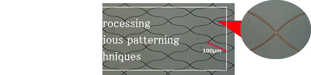
1.Patterning processing corresponding to any thin film
In partnership with multiple film-formation manufacturers, we are capable of patterning processing various thin films.

Please consult with us each specification of the multilayer film.
2.Available for small lot / quick delivery
We are available for customer's desired quantity / delivery time.

Processing lead time:3 days.

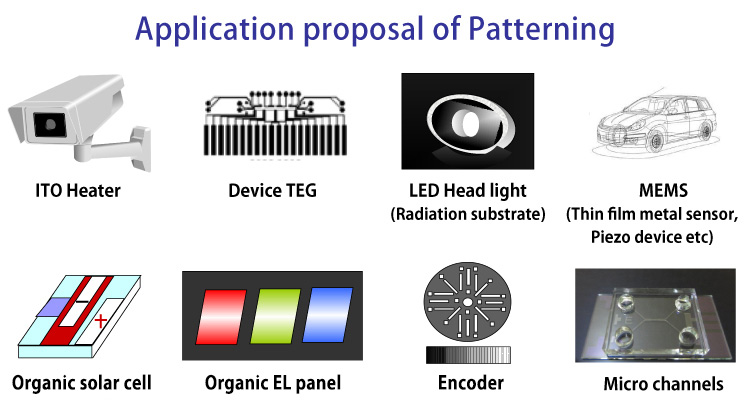
3.Example of applications
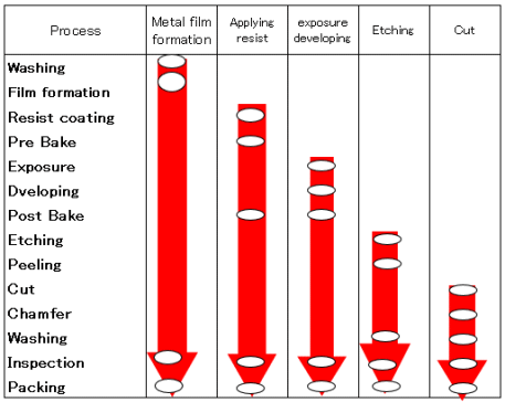
4.Processing technology

- Sealing cap
- Rrooved pattern
- Hole forming
- Putting film to glass substrate
- Adhering glass substrates together
- Cell production etc.
5.Cutting and slight chamfering
- Scribing
- Dicing
- Resist
- Ag electrode
- Insulating film, etc.
9.Glass cutting
- plain glass
- with thin film ( multilayer film ) attached
10.Patterning by means of lift off
12.ITO Heater
- Visible heaters like ITO are recommended
5.Assisting various materials evaluation
- I would like you only to apply our own resist.
- Is there any place you can ask for exposure and development only?
- I would like to peel film from substrate!
- I want to work in a clean room.
- I want to get a small glass as cheap as possible !


- In addition to full course from normal cleaning / resist coating to packaging,Cleaning / resist coating only, exposure / development only, etching ~ cut chamfering etc.
We also accept processing limited to.
* Perform resist coating, exposure and development under a clean room. - In order to evaluate the development of base materials such as PET and PEN, we will assist you with conditions such as resist and polyimide coating.
- Also we will create an evaluation report according to your request.
- In addition to helping with evaluation of small lot, please consult mass production correspondence.
 | |
 |  |
 |  |
 |  |
 |  |
 |  |  |
Click here for the main equipment
6.Substrate for equipment evaluation
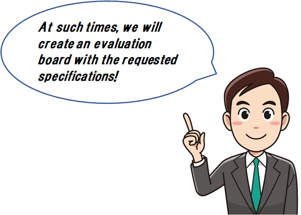
- Creating a performance evaluation board for optical equipment that requires pattern recognition
*For performance evaluation boards when considering the purchase of expensive equipment such as exposure machines - Creation of a glass substrate for evaluation of organic EL encapsulation equipment.
- Prototype supply of equipment evaluation boards even in small lots and in a wide variety of products
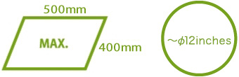
7.Target substrate / processing size
Target substrate

Maximum processing size
Key Track Records
Patterning commissioned for development or prototyping
| For LCD |
3D pattern Pattern for electronic paper Pattern for evaluation of liquid crystal material |
|---|---|
| For organic EL |
Pattern for lighting or display Glass cap for sealing Pattern for evaluation of organic EL material |
| For various TEGs | Pattern for evaluation of ACF,IC,FPC, or LCD |
| For various MEMS | Pattern for evaluation of sensors |
| For various Heaters | Pattern for evaluation of ITO for heaters |
| Pattern for solar cell | The organic thin film solar cell electrode pattern |
| Thin film coating substrate film | Organic EL・Organic solar cell・Electrochromic pattern |
| Optical test chart | The distortion of lens, optical characteristic evaluation |
| Biotechnology | Micro channel・cell culture pattern |
| For Encorder | Rotary・Liner Encorder |
| Evaluation support for development of various materials | New resist · Pattern condition of film such as PET, PEN etc. Evaluation support |
| Microstructure formation | Follow ability evaluation of adhesive, adhesive film, filler (semiconductor PKG etc.) Micro folder such as micro LED Cover glass spacer of solar cell etc. |


Please make use of our equipment according to your request.
In particular, the photolithography process works in a clean room (Class1000) environment.
* Furthermore, the coating process (roll coater), exposure equipment, etc. are further improved in cleanliness at the local booth (Class100).
| Process | equipment | Corresponding board size (mm) | Specifications / Remarks | |
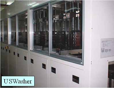
| Washing | washing machine | Batch type washer | MAX:420×530 | Alkaline, with US function |
| Single-wafer type washer | 67×105~530×920 | thickness to be put: 0.2t ~ 2.1t | ||
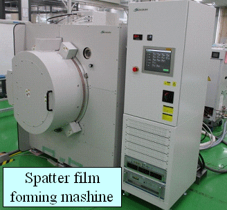
| Film formation | Film formation | Spatter film forming machine | MAX:210X300 | RF / DC power supply Reverse spattering possible |
| □MAX:270X270 | Corresponding TGT Cu, Ti, Cr, Ni, Au, Al, etc. | |||
| ~385φ | Film thickness approx. ± 10% | |||
| Photolithography | Coating (resist) | Roll coater | Effective width:100~550 | Resist thickness:1~2μm |
| Plate thickness:0.3~4 | ||||
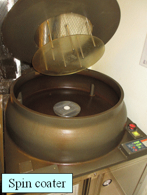
| Spin coater | φ20~300×400 | Rotational speed:300~2500rpm ±1rpm | ||
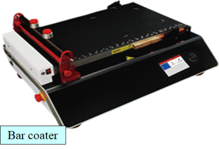
| Bar coater | MAX:300×400 | |||
| Screen printing | range:300×500 | Camera alignment accuracy±0.1㎜ | ||
| range:600×800 | ||||
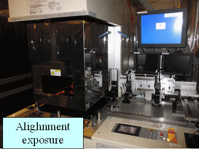
| exposure | Exposure machine | MAX300×400 | Alignment accuracy±1μm | |
| MAX400×500 | ||||
| developing | Single leaf type | 400×500 | Compatible with solvents and organic alkalis. | |
| Batch tank | 300×400 | |||
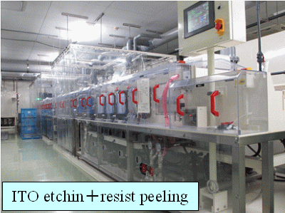
| etching | Wet etching | Single leaf type(ITO) | 420×530 0.2~2.8t | |
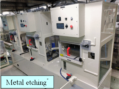
| Shower type(Cu,Al,Cr) | MAX:210X300 | *Cu,Al,Cr | ||
| Batch tank | 300×400 | * Please contact us for compatible membrane types. | ||
| Peel off (resist) | Batch tank | MAX370×470 | Alkaline type, organic solvent type | |
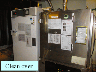
| Drying / baking | Oven | Clean oven | Inside:(W)800x(D)750x(H)1000 | Max350℃ Cleanliness class 100 N2 can be introduced |
| Hot plate | Hot plate | MAX300×400 | Max300℃ | |
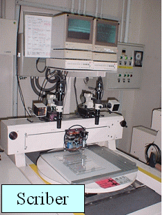
| Disconnect | Disconnect | Scriber | Max:500□ Max:3t | Cut accuracy±0.2mm |
| chamfer | Chamfering machine | 20□~300×400 | Consultation is required for board thickness | |
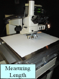
| Test | Measuring instrument | Stereomicroscope | ||
| Measuring microscope | ||||
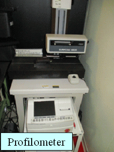
| Profilometer | ||||
| Transmittance measuring machine | ||||
| Digital force gauge | ||||
| Four probe tester | ||||
| Insulation tester | others | evaluation | Constant temperature bath | Inside:(W)400×(D)400×(H)400 | -85~180℃ |
| High temperature and humidity tank | Inside:(W)500×(D)600×(H)750 | -40~100℃ 20~98% | ||
| Stirring / defoaming | Stirring / defoaming machine | Max:250g | ||
| UV irradiation | Spot irradiator | |||
| Single-leaf irradiator | Effective width:250 | |||
| Repair | Laser repair machine | |||
| FPC crimping | FPC crimping machine | Effective width:30 | ||
| Effective width:100~300 | With alignment function | |||
| Pasting together | Film bonding machine | Adhesion accuracy:±0.2㎜ | ||
| Glass bonding machine | 200×300~360×400 | Alignment accuracy±0.1mm~ | ||
| Pressurized defoamer | Inside:(W)400×(D)500×(H)600 | |||
*Please contact us for details as all equipment depends on the material of the base material to be charged.
What is Photofabrication
Photofabrication is a type of manufacturing process that uses light to create minute structures and patterns.
It is mainly used in semiconductor manufacturing and microdevice manufacturing, and is important for efficiently and precisely manufacturing devices with fine structures.
The basic photo fabrication steps are as follows:
- Photoresist coating: A thin light-sensitive film called a photoresist is applied to the target substrate to form a pattern of light that is developed.
- Exposure: A light mask or optical system is used to project a specific pattern onto the photoresist.
- Development: The photoresist is immersed in a developer and the areas changed by exposure are removed, leaving behind the desired pattern.
- Etching or plating: Leaving areas protected by photoresist, areas removed by exposure may be etched or plated to form the final structure.
- Photoresist removal: Remove the remaining photoresist to obtain the final product.
Photofabrication is essential in the production of microstructured devices and integrated circuits, and has wide applications in semiconductor engineering and microdevice manufacturing technology.
Photofabrication process explanation (patterning)
(Example: single-layer ITO)
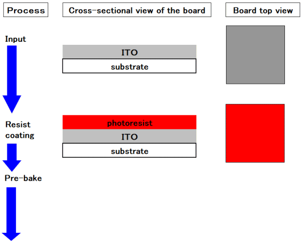
Forming a thin film resistor on the base material
- Substrate materials include glass, Si wafer, film, and others.
- Thin films can be laminated based on ITO, Cr, Al, etc. upon request.
(Consultation required)
Applying a material called resist that is exposed to UV light
- Can be coated with developed materials and polyimide.
- It is also possible to make different film thicknesses for each.
- Can also coat non-photosensitive materials
After applying the resist, light baking is performed at a low temperature
to dry the resist and make it adhere to the substrate.
However, it is dry enough to react with exposure and form a pattern.
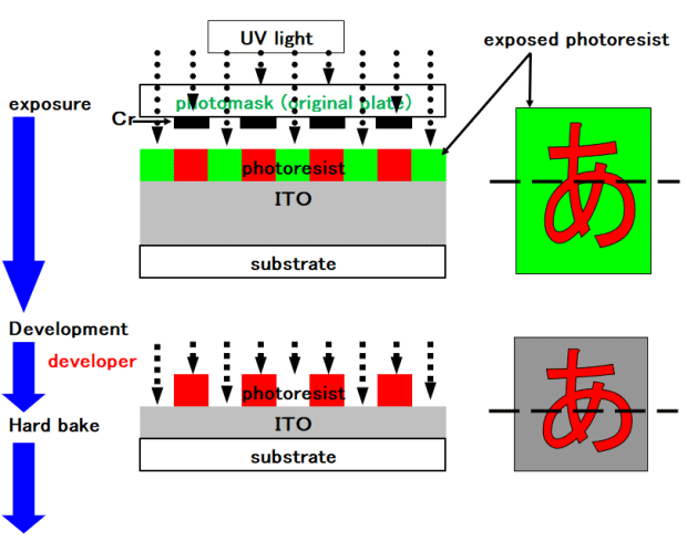
By applying UV light through a photomask (original plate), the resist changes in the areas exposed to UV light.
Positive type: The area exposed to UV light will dissolve in the developer.
Negative type: hardens where exposed to UV light
The developing solution (alkaline) dissolves the unnecessary parts of the resist,leaving only the parts where ITO is needed.
- Use organic or inorganic alkali depending on the type of membrane.
It is a process that stabilizes and hardens photoresist.
Main baking allows the photoresist to firmly adhere to the substrate,improving its durability during subsequent processes such as etching and plating.
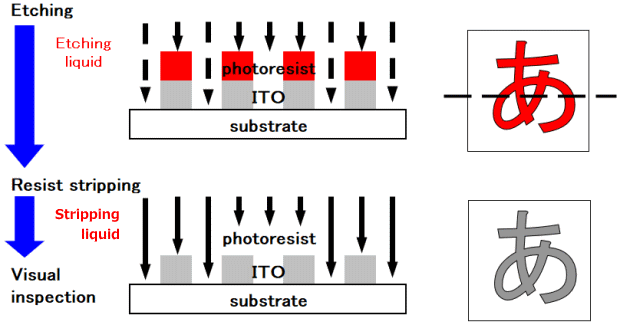
The desired shape can be obtained by using an etching solution to dissolve, erode, and etch the parts of the film that are not protected by the resist.
Decompose the photoresist with an alkali or solvent and remove it. The stripping solution is selected depending on the type of thin film.
Visually inspect, reject non-conforming products, pack and ship.