
Film formation processing
Until now, all the film formation processes had been processed by a partner company, but this time we have introduced a spatter film formation machine and it is
Features
Do you have such an experience when you requested the film formation process?

- "Oh No, can't you clean the board?"
- "Is the film formation condition only one condition per batch?”
- "Is the number of 1 batch fixed? 2 batches if the number increases even by 1?”
- "Well, does it take more than 2 months for delivery if you ask for film formation to patterning?"

- "Is there any place to handle from the arrangement of the glass substrate?"
- "Can you arrange from the glass substrate?"
- "Is there a place that can respond flexibly in small lots?”
- "Can I ask you to arrange a case after film formation?"
- "Is it possible to process everything from patterning after film formation to individual piece cutting in one go?"

Features of technoprint sputter film formation processing
- If necessary, we can clean the substrate before film formation.
- We will consider short delivery time for small lots. * Note 1
- The number of processed sheets can be flexibly handled from 1 sheet in small lots.
- We can flexibly handle from one small lot.
- It is also possible to notify the peeling test result after film formation and start processing. * Note 2
- We handle everything from film formation to patterning and individual piece cutting.
- Short delivery time can be achieved even with multilayer film patterning via an interlayer insulating film. * Note 3
- For sizes, film types, and quantities that cannot be handled by our company, we will cooperate with our partner companies.
* Note 1, 2, 3, there are conditions for compatible film types, sizes, and quantities, so please contact us for details.
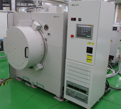
Spatter film forming machine
| Corresponding size(mm) | Specifications / Remarks | |
| MAX:210X300 ~385φ | RF・DC power supply・Reverse spattering possible | |
| Corresponding TGT | Cu・Ti・Cr・Ni・Au・Al・Mo・W APC‐TR・AlNd・MoNb・NiCr etc. | |
What is film deposition?
It is the process of attaching a thin film to the surface of a substrate such as glass, resin, metal, or paper.
By forming a film on the surface of a substrate such as an electronic device or semiconductor, it can protect the surface, conduct electricity, prevent electricity from passing, prevent reflections, and add various functions.
・Film formation method (typical example)
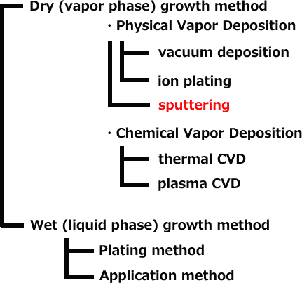
・sputtering(film formation method of TCN)
One of the methods for manufacturing thin films.
It is a method that uses glow discharge to cationize Ar, which hits the target at the cathode, knocking out particles from the target material and depositing the thin film on the substrate.
This process provides high film quality and uniformity and is suitable for forming fine structures and multilayer thin films. It is performed in a vacuum and can be applied to a wide range of materials such as films and ceramics, and has a wide range of applications such as MEMS/semiconductor manufacturing, display technology, and optical coatings.
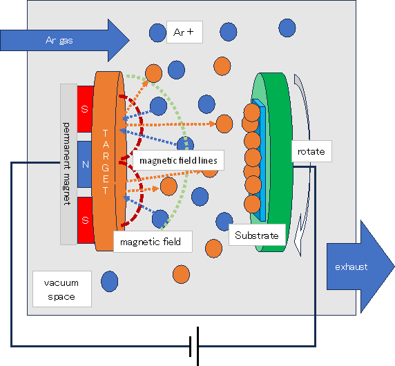
TCN uses the side sputtering method.