Technology Information
On this page we will introduce processing technology unique to techno print.
Plating process
Fine pattern formation by plating
There are various plating methods for Si wafers and glass substrates,
but Technoprint also specializes in thick film fine wiring patterns using electrolytic plating methods.
This method is suitable for 3D mounting and the high integration and miniaturization of semiconductor devices.
Handling substrates | glass substrates |
Size | 70mm□~200*300mm |
plating methods | Cu、Ni、Au etc |
Process Example
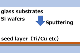
①Seed layer formation
Sputtering forms a seed layer on the surface required for electrolytic plating.
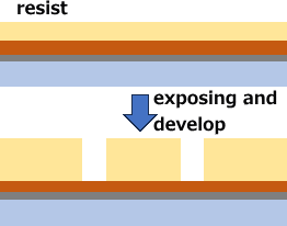
➁Photolithography
By applying resist to the entire surface of the base material,
exposing and developing it using a mask,
we create openings in the resist where
the plating process will be performed.
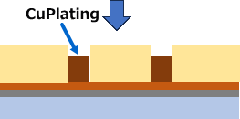
③Plating
Plating is grown in the opening while electricity is
passed through the power supply on the outer periphery
of the base material (electrolytic plating method).
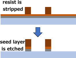
④resist is stripped and the seed layer is etched
After plating is complete,
the resist is stripped and the seed layer is etched
to form the final pattern.
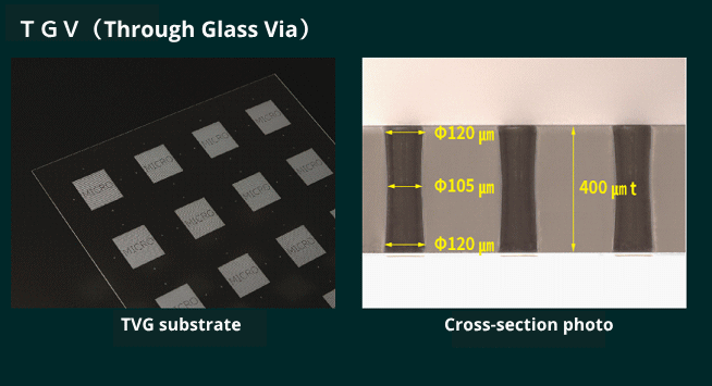
TGV(Through Glass Via)
TGV(Through Glass Via)
~Through Glass Via~
Applications: |
Multiple semiconductor chips with different functions can be mounted on a single substrate. |
Glass material: | Alkali-free glass, borosilicate glass, Tempax, synthetic quartz, etc. |
Glass thickness: | 0.1mm~1.0mm |
Via diameter: | Φ50μm~ |
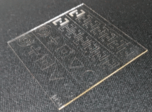
Fine metal mesh pattern processing
We support pattern processing of transparent fine metal mesh film.
Metal mesh film heater
Prevention of snow accretion and snow melting by using LED heads and rear lights instead of conventional halogens.
Measures against frost and snow melting on the windshield in front of the camera for automatic safety brakes for ADAS and autonomous driving.
Metal mesh film antenna
Supports 5G mini base stations and supports transparent antennas for buildings and vehicles.
Outer diameter of film substrate ~ A4 (PET / PC etc.) ... * Can be considered up to 300 x 300mm (conventional glass substrate can also be used)
2μm~ Cu wiring processing (consult us for conventional thin film patterning and plating build-up)
* L / S of the pattern depends on the film quality, thickness, length and shape of the base material and resist material.
* Please contact us for assistance in developing new materials for fine metal mesh processing.
Pattern examples Straight lines and corrugated shapes are also supported. (Enlarged view)

Transparent resist coating and patterning
Transparent resist coating and microfabrication patterning 2 μm-
specification | |
Pattern width | 2 μm- |
Film thickness | 0.6~30μm |
Coating size | Can be considered up to 300 x 300mm |
Application examples
・ Because it is insulative and transparent, it can be used as a protective film or interlayer insulating film for substrates instead of conventional Pi.
・Since it is photosensitive, partial patterning is possible.
・For resist for full additive plating for metal mesh film processing.
* The processing details depend on the length and shape of the pattern and the substrate quality.
* In the future, we will challenge L / S below 3μm, so please contact us.
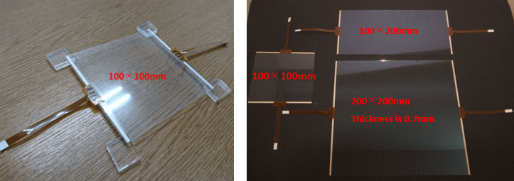
ITO heater standard sample product
We have prepared a standard sample of ITO heater which is frequently inquired.
External form: 100 x 100 x 0.7 mm, 100 x 200 x 0.7 mm, 200 x 200 x 0.7 mm
Resistance value about 10Ω ・ 45Ω ・ 85Ω
Terminal treatment Ag paste, with or without FPC (ACF crimping)
*Price, please contact us.
* Please contact us for availability.
* Please use this product for initial evaluation and evaluate the long-term reliability under your environment.
* Can be customized based on this sample.
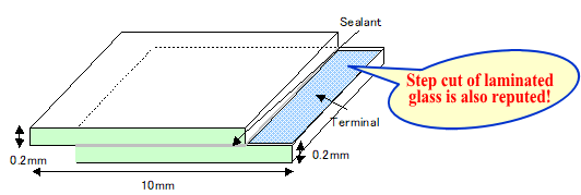
Empty cell(Thin glass laminatinging process technology)
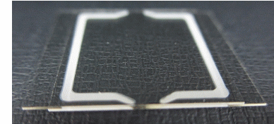
We will help you create empty cells etc with thin glass laminating technology cultivated with glass / glass touch panel.
①Processing contents
・Glass + glass laminate(Can step cut). Glass + film lamination (Specification consultation necessary)
②Processing size
・MAX It is possible to process glass substrates up to 400 mm × 360 mm.Thinness up / down 0.2mm ~Available
G+F:(Specification consultation necessary )
③Machining record
・Gap between glass and glass:10~30μm(Bonding with sealing material)
MEMS(Thin film metal sensor processing)・・・Alcohol breath sensor
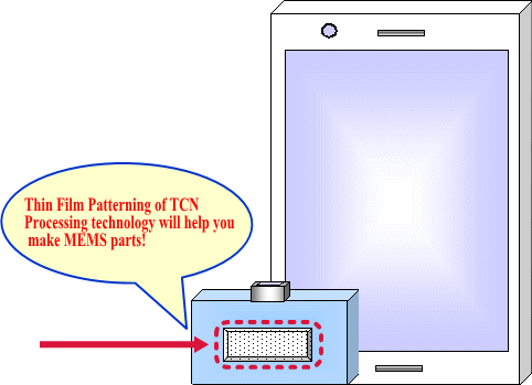
Patterning technology for multilayered thin film of Techno print contributes to processing of MEMS sensor parts.
* Patterning of metal thin film and coated insulating film realizes sensor part and its heater function.
Furthermore, sensors can be miniaturized as individual sides.
Illustration is an alcohol breath sensor linked with a smartphone.
* The real thing and the image are different.
Electrochromic・・・NIMS・WASEDA・TAMA Art University Joint development project
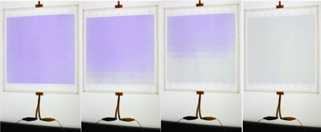
An electrochromic type light control glass that can change light shielding state by applying electricity has been used for windows of airplanes and the like in recent years.
However, until now, there is no choice but to adjust the light shielding condition throughout the glass, and after shading it was impossible to enjoy the view outside the window.
This time, the research group developed a light control glass that changes the gradation using a polymer (organic / metal hybrid polymer) with electrochromic properties that we have studied so far.
Detail is here.
Techno print thin film processing technology is also utilized for pattern development and patterning processing on the ITO film formed on the glass of this product.
It was also featured on World Business Satellite "Tretama" broadcast on December 19, 2019.
ITO heater processing
It contributes to product making even by ITO patterning and Outline processing, and ACF crimping of wide FPC.
principle
When the electrode is energized, Joule heat is generated in the transparent conductive film,
heated with the glass, far infrared rays are emitted from the glass surface.

Size
Panel shape: minimum 10 mm x 10 mm to maximum 370 mm x 470 mm. Wafer shape: minimum to maximum 300 φ

Application
・For dew condensation prevention of surveillance cameras and equipment requiring visibility
・Micro flow path etc Want to warm while observing Chemical analysis, for cell culture experiment!
・For aircraft and special vehicle monitors that require full LCD performance!
・To prevent fogging of the mirror in the bathroom and the washroom!
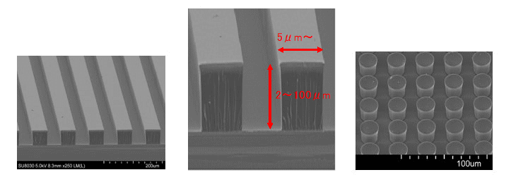
Formation of fine structure
At TCN, we provide customized types of μm precision with various resist agents.
Pattern shape can be straight / circular (cylindrical)
Aspect ratio 5: 1 (film thickness 50 μm or more) possible, (3: 1 actual results)
- I want a rectangular unit of μm in base with good accuracy, where should I order?
- Where is the place customized even in small quantities?
- I want you to customize various heights and shapes!

Application example
Evaluation of tracking performance of adhesive, adhesive film, filler (inside of semiconductor PKG, etc.)
Micro folder such as micro LED
Cover glass spacer for solar cells etc.
In addition to simulation, evaluation and verification that is close to the actual machine is possible.
By creating a mask, it is possible to divide multiple shapes by changing the line width such as L shape, straight line, circular shape (cylindrical) etc. on the same board.
Aspect ratio 5: 1 (film thickness 50 μm or more) possible, height 2 to 100 μ possible
* However, the same height is on the same board.
Substrate size is easy to use up to 300 mm in large format □ 50, 100, 200 mm and any size can be cut.
Glass / silicon wafers etc are possible as base material.
